intel 8255 pin diagram

PA0- PA7: port a, it is 8 bit bi-directional i/o pins.
PB0-PB7: port b, It is 8 bit bi-directional i/o pins.
PC0-PC7: port c, It is also a bi-directional i/o pins. It is divided in two sections: PC0-PC3 and PC4-PC7. These two section can be used to transfer 4 bit data.
D0-D7: data pins for data transfer
RESET: reset input, It is used to reset 8255 ic.
RD-bar: read input, it is used to coordination with other signals to send data through data lines.
WR-bar: write input, used in coordination with other signals to send data to 8255.
A1-A0: address pins
00-Port A
01-Port B
10-Port C
11-Control Reigster
CS-bar: chip select
Tag :
8255PPI
8255 block diagram

It has been divided in two section: Group A and Group B. Each of 12 bits.
Group A: PA0-PA7 & PC4-PC7(port C upper)
Group B: PB0-PB7 & PC0-PC3(por C lower)
Each group can be programmed separately.
The GA and GB control block receives commands from r/w control logic to accept bit pattern from CPU.
GA(Group A) controls GA ports and GB controls GB ports.
The function of port a and port b is decided by the control bit pattern available in GA and GB control register.
Function of port a and b are also dependent on the mode of operation.
Port C can be programmed separately for port c upper and port c lower.
The port C function is also dependent on the mode of operation.
It can be used as simple i/o, handshaking signals and status signal inputs.
Tag :
8255PPI
8255 programmable periferal interface
8255 is a programmable peripheral interface.
It contains three i/o port that can be programmed in
different mode.
It is a general purpose programmable parallel i/o device.
It contains s a control register that can be programmed to
control the function of port as well as it can also control that which mode
they should operate.
It is a programmable parallel i/o device.
It consists of three input/output ports each of 8 bits. It
has been arranged as two 8 bit ports and two 4 bit ports.
It has been arranged in two groups each of 12 bits.
It is TTL compatible also.
It also provides facility for the direct set and reset for
port C.
It can operate in three modes:
1 Mode 0
2 Mode 1
3 Mode 2
Tag :
8255PPI
8155 Timer
The 8155 timer consists of two 8-bit registers.
1. 8-bit LSB and 8-bit MSB.
2. In these 16 bits, 14 bits are used for counter and two bit for mode selection.
3. The counter is a 14 bit down counter. It can operate in 4 different modes of operation.
Timer MSB:
|
|||||||
M2
|
M1
|
T13
|
T12
|
T11
|
T10
|
T9
|
T8
|
Timer LSB:
|
|||||||
T7
|
T6
|
T5
|
T4
|
T3
|
T2
|
T1
|
T0
|
We can select mode using two bits M2 and M1.
M2 M1
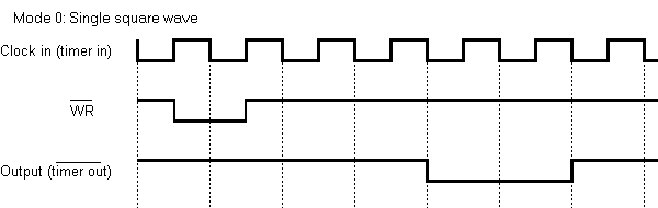
00(Mode 0)- Single Square Wave
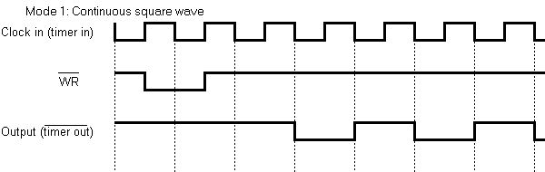
01(Mode 1)- Square Wave
10(Mode 2)- Single Pulse on TC(terminal count)
11(Mode 3)- Pulse every TC
Mode 0: In this mode, timer gives only one cycle of square wave, the output remains high for 1/2 count and remain s low for 1/2 count. If count is odd it remains high for (n+1)/2 and low for (n-1)/2. Where n is count value. Wave width depends on two factor: one is Input clock pulse frequency, and the other is count loaded in counter.
Mode 1: This mode is similar to single square wave in operation but the when counter becomes zero, the count value is automatically reloaded. Thus it provides continuous square wave.
Mode 2: This mode gives a single clock pulse as a output of the end of the count.The output is high normally, but it becomes low for 1 clock pulse and again it will become high and remain high.
Mode 3: This mode is similar to mode 2 but when the counter becomes zero the count value is automatically reloaded. Thus it provides continuous pulses.
Tag :
8155 PPI